Application Notes

Application Notes

Super-Resolution Microscopy (STED and PALM)

One super-resolution approach is called stimulated emission depletion (STED) microscopy. This technique uses a confocal microscope and a diffraction limited excitation beam that is …

Application Notes

Flat Panel Display Manufacturing

As the flat panel display market moves from LCD to OLED display technology, laser patterning and cutting of heterogeneous materials (comprised of multiple organic material films) with …

Application Notes

Solar Panel Manufacturing

Crystalline-Silicon solar cells are the predominant solar cell technology used in fabricating solar panels because of the availability of silicon, well-developed manufacturing processes, …

Application Notes

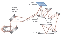
Deep UV Photolithography

DUV technology for photolithography is exclusively based on projection optics since the pattern on the photomask is much larger than the final pattern developed on the photoresist.

Application Notes

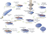
Semiconductor Manufacturing Overview

This application note provides a brief overview of semiconductor manufacturing and describe the various optical techniques used to define, inspect, and measure feature sizes and layer …

Application Notes

Laser Micromachining

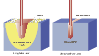
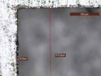
Laser machining is a non-contact process that can achieve higher precision and quality, smaller features, improved consistency with no tool wear, and possesses the flexibility to machine …

Application Notes

Real-Time Laser Power Measurement

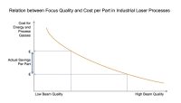
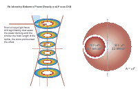
Only when performing optimally can laser systems guarantee the most cost-effective production of high-quality components. Even the smallest deviations in beam adjustment or focal position …

Application Notes

Thermal Imaging

Thermal imaging techniques involve discriminating between various objects in a scene based on their respective differences in temperature.

Application Notes

Photoacoustic Microscopy (PAM)

Unlike the pure optical microscopy techniques, PAM takes advantage of the weak acoustic scattering in tissue and thus breaks through the optical depth penetration limit (~ 1 mm) in …

Application Notes

Three-Photon Fluorescence Microscopy (3PF)

Three-photon fluorescence (3PF) microscopy can provide a significant advantage over 2PF microscopy in strongly scattering samples such as the mouse brain.

Application Notes

Optogenetics

Optogenetics combines genetic and optical techniques to selectively and specifically modulate signaling pathways in intact living organisms using light.

Application Notes

MALDI Time-of-Flight Mass Spectrometry

MALDI is a soft ionization technique used in mass spectrometry (MS) that produces rapid and efficient ionization of a wide variety of molecules.

Application Notes

Powder Bed Fusion

Powder bed fusion systems utilize a heat source—such as a laser—to sinter or melt ultra-fine layers of material like powdered metal to fuse into the desired shape.

Application Notes

Vat Polymerization

In vat polymerization systems—including stereolithography (SLA) and digital light processing (DLP)—a UV laser constructs an object in a vat of a liquid photopolymer resin by curing …

Application Notes

Tunnel Oxide Passivated Contact (TOPCon) Processing

One technology which shows promise of meeting the growing demands of solar panel quantity, performance and cost-effectiveness is TOPCon, or tunnel oxide passivated contact, technol …

Application Notes

Ophthalmic Surgery

Ophthalmology is the branch of medicine that deals with the anatomy, physiology and diseases of the eye. The laser is particularly suited to ophthalmic surgery since it can provide …

Application Notes

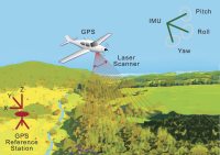
LiDAR

LiDAR is an active remote sensing technique that is similar to RADAR but, instead of using radio waves as a radiation source, it uses laser pulses. In this technique, a laser source …

Application Notes

PCB Manufacturing

Lasers are routinely used in a variety of PCB manufacturing processes including via drilling, depaneling, profiling, laser direct imaging, repair, trimming, and marking. Laser processing …

Application Notes

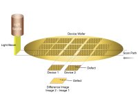
Semiconductor Inspection

In this application note, we provide a brief description of the basics of wafer and reticle inspection techniques and discuss the characteristics of current inspection tools.

Application Notes

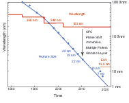
Semiconductor Lithography Overview

Lithography is defined as "a method of printing from a flat surface (such as a smooth stone or a metal plate) that has been prepared so that the ink will only stick to the design that …

Page 1 of 8